- Motorola Edge 30 Neo - wake up, Jr...
- Samsung Galaxy Watch (Tizen és Wear OS) ingyenes számlapok, kupon kódok
- Samsung Galaxy A54 - türelemjáték
- Magisk
- Samsung Galaxy A52s 5G - jó S-tehetség
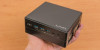
- Poco X6 Pro - ötös alá
- Xiaomi Redmi Note 4 - B20
- Honor Magic V2 - origami
- Dobhatja a Google az Exynost és a Samsungot
- Mobil flották
Hirdetés
-

Computex 2024: gamer alaplap és „AI” PC az ECS-től
ph Az Elitegroup új LIVA barebone-nal és a Black alaplapsorozat feltámasztásával készül a tajvani kiállításra.
-


Tekken 8 - Nyáron érkezik Lidia Sobieska
gp A lengyelek karatézó vezére lesz a franchise nyolcadik részének legújabb DLC karaktere.
-


Az Amazon eurómilliárdokat hozna az olasz és az európai felhőbe
it A jelentések szerint Olaszországgal folytat megbeszéléseket az Amazon a több milliárd eurós befektetésről.


Új hozzászólás Aktív témák
-

Kígyószem
csendes tag
válasz
 Vakegérke
#4172
üzenetére
Vakegérke
#4172
üzenetére
most töltöttem le RAMMON progit ,ott valamiket ki írt ,csak nem tudom miket , majd jövő héten meg csinálom mert rossza pendrivém , igen használok most is gépet,csak nem jó a dvd írom ,úgy szoktam kölcösn kérni havertól
de szerintem olyan ramot kell bele vennem amit támogat is
ezeket írja ki :
Ram Type DDR DDR
Maximum Clock Speed (MHz) 200.00 (JEDEC) 200.00 (JEDEC)
Maximum Transfer Speed (MHz) DDR-400 DDR-400
Maximum Bandwidth (MB/s) PC3200 PC3200
Memory Capacity (MB) 512 512
Jedec Manufacture Name Kingmax Semiconductor Samsung
Search Amazon.com Search! Search!
SPD Revision 0.0 0.0
Registered No No
ECC No No
DIMM Slot # 1 2
Manufactured Week 1 of Year 2005
Module Part # MPXC22F-D8KT4B M3 68L6423FTN-CCC
Module Revision 0x0 0x4E46
Module Serial # 0x0 0xFB9A08F1
Module Manufacturing Location 65 2
# of Row Addressing Bits 13 13
# of Column Addressing Bits 11 10
# of Banks 4 4
# of Ranks 1 2
Device Width in Bits 8 8
Bus Width in Bits 64 64
Module Voltage SSTL 2.5V SSTL 2.5V
CAS Latencies Supported 2.0 2.5 3.0 2.5 3.0
Timings @ Max Frequency (JEDEC) 3-4-4-8 3-3-3-8
Maximum frequency (MHz) 200.00 200.00
Maximum Transfer Speed (MHz) DDR-400 DDR-400
Maximum Bandwidth (MB/s) PC3200 PC3200
Minimum Clock Cycle Time, tCK (ns) 5.000 5.000
Minimum CAS Latency Time, tAA (ns) 15.000 15.000
Minimum RAS to CAS Delay, tRCD (ns) 20.000 15.000
Minimum Row Precharge Time, tRP (ns) 20.000 15.000
Minimum Active to Precharge Time, tRAS (ns) 40.000 40.000
Minimum Row Active to Row Active Delay, tRRD (ns) 10.000 10.000
Minimum Auto-Refresh to Active/Auto-Refresh Time, tRC (ns) 60.000 55.000
Minimum Auto-Refresh to Active/Auto-Refresh Command Period, tRFC (ns) 70.000 70.000
DDR1 Specific SPD Attributes
Data Access Time from Clock, tAC (ns) 0.700 0.650
Clock Cycle Time at Medium CAS Latency (ns) 6.000 6.000
Data Access Time at Medium CAS Latency (ns) 0.700 0.700
Clock Cycle Time at Short CAS Latency (ns) 7.500 0.000
Data Access Time at Short CAS Latency (ns) 0.750 0.000
Maximum Clock Cycle Time (ns) 12.000 10.000
Address/Command Setup Time Before Clock, tIS (ns) 0.600 0.600
Address/Command Hold Time After Clock, tIH (ns) 0.600 0.600
Data Input Setup Time Before Strobe, tDS (ns) 0.400 0.400
Data Input Hold Time After Strobe, tDH (ns) 0.400 0.400
Maximum Skew Between DQS and DQ Signals (ns) 0.400 0.400
Maximum Read Data hold Skew Factor (ns) 0.500 0.500
CS Latencies Supported 0 0
WE Latencies Supported 1 1
Burst Lengths Supported 2 4 8 2 4 8
Refresh Rate Reduced (7.8us) Reduced (7.8us)
Buffered Address/Control Inputs No No
On-card PLL No No
FET Switch On-card Enable No No
FET Switch External Enable No No
Differential Clock Input Yes Yes
Weak Driver Included No No
Concurrent Auto Precharge Supported No Yes
Fast AP Supported No Yes
Module Bank Density 512 MB 256 MB
Module Height (mm) Unavailable Unavailable[ Szerkesztve ]


Új hozzászólás Aktív témák

Állásajánlatok

Cég: Promenade Publishing House Kft.
Város: Budapest

Cég: Ozeki Kft.
Város: Debrecen