Hirdetés
- Samsung Galaxy S24 Ultra - ha működik, ne változtass!
- iPhone topik
- Samsung Galaxy A54 - türelemjáték
- Sony Xperia 1 V - kizárólag igényeseknek
- Sportfülhallgató futott be a Nothingtól
- Derült égből villámcsapásként itt a Galaxy S24 FE
- Vodafone mobilszolgáltatások
- Magyarországra is megérkezett a Xiaomi Smart Band 9
- Mobil flották
- Xiaomi 13T és 13T Pro - nincs tétlenkedés
Hirdetés
-
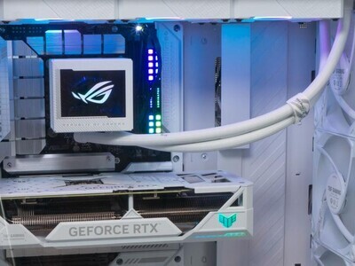

ASUS BTF koncepció: látszólag vezetékek nélküli PC
ph Összeépítettünk egy komplett rendszert a kábelezést az alaplap mögé száműző BTF megoldással.
-


Magyarországra is megérkezett a Xiaomi Smart Band 9
ma A fitneszkarkötő júliusban bemutatott legújabb generációja hazánkban is elérhető.
-


A felhasználók követése miatt bepanaszolták a Mozillát
it Adatvédelmi panaszt tett az osztrák NOYB a Mozillára a firefoxos felhasználók követése miatt.


-

Mobilarena
A legtöbb kérdésre (igen, talán arra is amit éppen feltenni készülsz) már jó eséllyel megtalálható a válasz valahol a topikban. Mielőtt írnál, lapozz vagy tekerj kicsit visszább, és/vagy használd bátran a keresőt a kérdésed kulcsszavaival!

Új hozzászólás Aktív témák
-
#37409
 Raymond
félisten
Alogonomus
#37404
Raymond
félisten
Alogonomus
#37404
Raymond
félisten
válasz
 Alogonomus
#37404
üzenetére
Alogonomus
#37404
üzenetére
Abban a tablazatban hatulrol (az 5nm-rol) indulnak egy bizonyos spec chip-el es a nagyobb node-oknal aszerint szamoljak mennyi jonne ki egy wafferbol hogy mekkora lenne az a chip az adott node-on az 5nm-hez kepest:
Chip transistor density. Our model uses, as a baseline, a hypothetical 5 nm
GPU with the specifications of Nvidia’s Tesla P100 GPU, which OpenAI used
in 2018 to train the breakthrough AI algorithm OpenAI Five. 191 The P100
GPU is fabricated at TSMC at the 16 nm node and contains 15.3 billion
transistors in a chip (die) area of 610 mm2 , translating to a transistor density
of 25 MTr/mm2 . 192 A 300 mm diameter silicon wafer produces 71.4 610
mm2 GPUs on average. 193 Our hypothetical 5 nm GPU has a chip area of
610 mm2 and given its greater transistor density than the P100 GPU, 90.7
billion transistors. 194 Table 7 presents estimated TSMC transistor densities for
nodes between 90 and 5 nm. For nodes in the 90 to 7 nm range, our model
uses a hypothetical GPU with identical specifications, including transistor
count, as the hypothetical 5 nm GPU, except with a transistor density
associated with the hypothetical node. Therefore, GPUs with nodes larger
than 5 nm will respectively have an area greater than 610 mm2 , resulting in
differing numbers of GPUs fabricated per wafer as shown in Table 7.
However, the model could equivalently be interpreted as accounting for one
chip at the 5 nm node, but at any given larger node, multiple chips totaling
the same transistor count as one 5 nm chip.Forras: az itt letoltheto PDF 41. oldala [link]
Privat velemeny - keretik nem megkovezni...


Új hozzászólás Aktív témák
A topikban az OFF és minden egyéb, nem a témához kapcsolódó hozzászólás gyártása TILOS!
MIELŐTT LINKELNÉL VAGY KÉRDEZNÉL, MINDIG OLVASS KICSIT VISSZA!!
A topik témája:
Az NVIDIA éppen érkező, vagy jövőbeni új grafikus processzorainak kivesézése, lehetőleg minél inkább szakmai keretek között maradva. Architektúra, esélylatolgatás, érdekességek, spekulációk, stb.


Állásajánlatok

Cég: Ozeki Kft
Város: Debrecen

Cég: Ozeki Kft
Város: Debrecen